Are blind vias more expensive
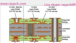
Blind vias are connections between layers of a PCB, and they conserve space compared to through-hole (PTH) vias. They are used in high-density interconnect PCBs, such as those found in tablets, laptops, and cell phones, to maximize function within a smaller area. While they offer many benefits, blind vias can also present challenges when designing and manufacturing a circuit board.
They can increase the amount of traces on the surface of a PCB. This allows for more functionality, but it can also result in a higher cost, especially when the number of traces is increased to a point where they start running into each other and creating crosstalk and EMI between signals. Fortunately, there are several ways to minimize the effects of this crosstalk and EMI while using blind via.
The first is to make sure that the holes are drilled at the correct depth. If the hole is too shallow, it can cause signal distortion or degradation. It can also lead to an improper connection with the adjacent layer. Luckily, it is easy to avoid these problems by using the proper drilling parameters in your design software.
Are blind vias more expensive to manufacture than through vias?
Another way to prevent this problem is to drill the blind via to the side instead of in the center. This will reduce the chances of a bubble forming beneath the solder ball, which can cause problems during the assembly process. It also helps to keep the copper in the hole as short as possible, reducing the potential for failure.
Lastly, it is important to use the correct plating process when using blind vias. This is because if the plating process runs too long, it can ruin the copper and cause the holes to become unusable. It is important to follow the manufacturers’ guidelines and always verify that the correct settings are being used.
In addition to minimizing the risk of failure, blind and buried vias also provide other advantages to the designer. They are less expensive to manufacture than buried vias because they do not require the same level of precision during the fabrication process. They are also less prone to mechanical errors, like drill breakouts and other defects that can occur in boards with through-hole vias.
However, despite the advantages that blind and buried vias offer, it is still important to use through-hole vias whenever possible. They provide a more reliable and stable connection between layers and can significantly reduce the overall cost of a circuit board. If you are considering adding through-hole vias to your PCB design, be sure to talk with a professional to ensure that the design is correct and that the proper techniques are being used. Contact an Altium expert today to learn more about the best methods for adding through-hole and blind/buried vias to your design.