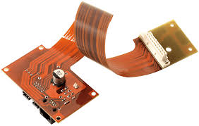
Can flex circuit pcb be used
Flex circuit PCBs, renowned for their flexibility and compactness, have revolutionized the realm of electronic design and manufacturing. Their unique ability to conform to complex shapes and tight spaces makes them ideal for a wide range of applications, from consumer electronics to aerospace systems. However, a common question that arises is whether flex circuit PCBs are suitable for high-frequency applications where signal integrity and transmission performance are paramount.
The answer to this question lies in understanding the characteristics of flex circuit PCBs and how they behave at high frequencies. Flex circuits, typically constructed from thin layers of polyimide or polyester substrates, offer excellent electrical insulation and mechanical flexibility. However, their electrical properties, such as dielectric constant, loss tangent, and impedance, can vary depending on the specific materials and construction techniques used.
In high-frequency applications, where signals operate at frequencies above a few megahertz, maintaining signal integrity becomes increasingly challenging. Factors such as signal attenuation, impedance mismatch, and electromagnetic interference (EMI) can degrade the performance of the circuit and compromise the reliability of the system. Therefore, selecting the appropriate materials and design considerations are crucial when using flex circuit pcb in high-frequency applications.

Can flex circuit pcb be used in high-frequency applications?
One of the key considerations for high-frequency flex circuit PCBs is the choice of substrate material. Polyimide and polyester films, commonly used in flex circuits, offer relatively good electrical properties and can be suitable for moderate-frequency applications. However, for high-frequency applications exceeding several gigahertz, specialized materials such as liquid crystal polymer (LCP) or polytetrafluoroethylene (PTFE) may be preferred due to their lower dielectric loss and higher signal integrity.
Additionally, the design and layout of flex circuit PCBs play a significant role in their suitability for high-frequency applications. Factors such as trace geometry, impedance control, and grounding techniques must be carefully optimized to minimize signal distortions and ensure consistent transmission performance across the frequency spectrum. Employing controlled impedance routing techniques and minimizing signal reflections can help mitigate impedance mismatches and ensure proper signal propagation.
Furthermore, the integration of shielding techniques is essential to mitigate electromagnetic interference and maintain signal integrity in high-frequency flex circuit PCBs. Utilizing ground planes, shielded traces, and RF shielding enclosures can help minimize electromagnetic emissions and susceptibility to external interference, thereby enhancing the overall performance and reliability of the circuit in high-frequency environments.
It’s also important to consider the fabrication process and its impact on the electrical properties of flex circuit PCBs in high-frequency applications. Factors such as copper thickness, surface roughness, and plating techniques can affect the conductivity and impedance characteristics of the circuit traces, influencing signal transmission and reception. Therefore, employing high-precision fabrication processes and ensuring tight quality control are essential to achieving optimal performance in high-frequency flex circuit PCBs.
In conclusion, while flex circuit PCBs offer numerous advantages in terms of flexibility and space savings, their suitability for high-frequency applications depends on various factors such as substrate material, design considerations, shielding techniques, and fabrication processes. With careful consideration of these factors and proper engineering practices, flex circuit PCBs can indeed be utilized effectively in high-frequency applications, delivering reliable performance and robust signal integrity.


